


The company claims that the new HBM chip will boost system performance by two times, while reducing energy consumption by over 70%
The HBM-PIM is currently being tested inside AI accelerators by the company’s AI solution partners. (Credit: SAMSUNG)
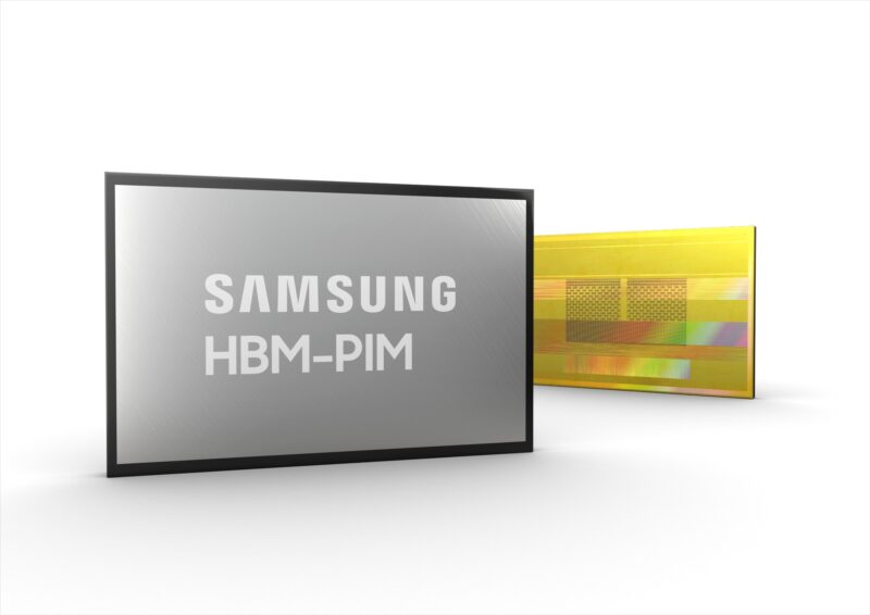
Samsung Electronics has developed a high bandwidth memory (HBM) chip dubbed as HBM-PIM, which has been integrated with artificial intelligence (AI) processing power.
By using the processing in memory (PIM) technology, the new architecture when applied to the company’s existing HBM2 Aquabolt solution is claimed to provide over twice the system performance.
The new HBM chip can also reduce the consumption of energy by over 70%, claimed the company.
Samsung Electronics said that the AI computing capabilities embedded inside the high-performance memory chip will help in speeding up large-scale processing in data centres, high-performance computing (HPC) systems, and also in AI-enabled mobile applications.
Samsung Electronics memory product planning senior vice president Kwangil Park said: “Our groundbreaking HBM-PIM is the industry’s first programmable PIM solution tailored for diverse AI-driven workloads such as HPC, training and inference.
“We plan to build upon this breakthrough by further collaborating with AI solution providers for even more advanced PIM-powered applications.”
According to the South Korean company, most of the computing systems that are used currently are based on the von Neumann architecture.
The systems use a separate processor and memory units to execute millions of intricate data processing tasks.
The company said that the sequential processing approach needs data to move back and forth constantly, which leads to a system-slowing bottleneck.
On the other hand, the HBM-PIM by placing a DRAM-optimized AI engine inside each memory bank can provide processing power directly to where the data is stored. This will facilitate parallel processing, while minimising movement of data, said Samsung Electronics.
Currently, the HBM-PIM chip is being put to test inside AI accelerators by the company’s AI solution partners. All the validations of the chip are anticipated to be completed within the first half of 2021, said Samsung Electronics.
Argonne computing, environment, and life sciences associate laboratory director Rick Stevens said: “I’m delighted to see that Samsung is addressing the memory bandwidth/power challenges for HPC and AI computing.
“HBM-PIM design has demonstrated impressive performance and power gains on important classes of AI applications, so we look forward to working together to evaluate its performance on additional problems of interest to Argonne National Laboratory.”